Project 1: Rationally Designed Photocatalytic Systems
Current photocatalysts are generally obtained by randomly loading metallic nanoclusters onto the surface of semiconductor particles as shown in Fig. 1A. The photoexcited electrons and holes randomly diffuse towards the surface of the semiconductor materials and promote surface photochemical reactions. Unfortunately, the random movement of electrons and holes will lead to their recombination. Therefore, a majority of the photogenerated electrons and holes are not utilized. Moreover, photochemical reactions directly happening on the surface of the semiconductor materials may cause the semiconductor to degrade more readily. My group will rationally design novel nanostructures with high quality interface which can favor the electron-hole separation and transportation. The pure water splitting and CO2 reduction are the emphasis of my research group. A typical design is displayed in Fig. 1B, in which the integration of semiconductor as light absorption antenna and metals as catalysts is encased inert shell. In such a structure, the interface with high quality is desired for highly efficient solar energy conversion. The multi-junctions including tandem structures will be synthesized and used for solar energy conversion as shown in Fig. 1C.
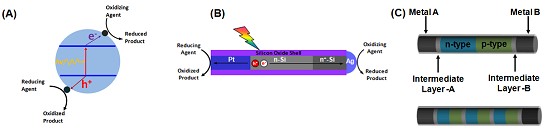
Fig. 1 (A) Schematic of photocatalytic process; (B) A typical design photocatalysts with high efficiency and stability. (C) Proposed photodiodes as photocatalysts.
Project 2: Integrating Nanostructures with Membrane for Water Splitting
On the basis of Project 1, the high quality heterogeneous nanowires could be synthesized with controllable chemical and physical properties. Especially, achieving photoelectric nanodevices with larger built in potential will be important to artificial photosynthesis including direct water splitting. In the future, separated reactors for reduction and oxidization reaction will be considered due to two concerns: (1) Separation of oxidized and reduced products and (2) Optimized reaction conditions for oxidization and reduction, respectively. A membrane-based reactor is shown in Fig. 2A and 2B. Fig. 2A shows a structure of nanowire array embedded in proton exchange membrane. Fig. 2B represents thin film technology using nanowire array as template. The membrane should satisfy three requirements: (1) optically transparent to incident light, (2) good chemical stability, and (3) excellent adhesion to the photocatalysts. Polydimethylsiloxane (PDMS) is a potential candidate for such applications.
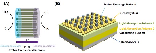
Fig 2. (A) Schematic of Heterogeneous Nanowires integrated with proton exchange membrane for water splitting. (B) Schematic of multilayer thin film using nanowire array as template for water splitting and electrochemical synthesis.
Project 3: Surface Plasmon Resonance (SPR) of Metal Nanostructures in Novel Solar Cell
Employing SPR effect of metal nanostructures potentially can reduce the 10 folders or even 100 folders of the semiconductor materials to achieve comparable light absorption of its counterpart. Such a thin solar cell has the potential to improve the efficiency of solar cell, especially for organic polymer based solar cell. The light absorption depth for most organic semiconductors is ~10 times larger than the exciton diffusion length. The internal quantum efficiency of organic PVs decreases quickly with increasing film thickness due to (1) only a small fraction of generated excitons diffusing to the interface of the donor and the acceptor and (2) loss of charge carriers to recombination during transport. Therefore, one promising solution is to investigate ultrathin organic solar cells using SPR effect of metal nanostructures. This effect can be extended to Multiple Exciton Generation (MEG) Devices and organic-inorganic hybrid solar cell.
Project 4: Functionalized Nanostructures for Chemical Sensors and Bio-Sensors
Chemical sensor is to provide real-time reliable information about the environment of its surroundings. Ideally, such a device is capable of responding continuously and reversibly and does not perturb the sample. Such devices consist of a transduction element covered with a biological or chemical recognition layer. Recently, nanostructured materials have attracted considerable intentions for various applications due to their unique physical and chemical properties compared to their counterparts. For example, the absorption of the metal and semiconductor nanoparticles is determined by the size of the nanostructures, which could be used to for the chemical and/or bio-sensors through color change observed by the naked eyes. The large surface areas of the nanostructures provide more surface areas for the accessory of the chemical and/or bio- species. Combining other features of the nanostructures, such as the high surface chemical activity and photo- and electro-luminescence, the nanostructures could be widely used for chemical- and bio- sensor. My lab will focus on using carbon-based nanostructures for bio- and chemical sensors.